Clock carrier
and clock-driver
modules.
The
function of generating clocks for an array is put on modules that
eventually are plugged together on a clock-driver carrier board. The
reason for
this is to be able to mix different types of modules. F.ex. in a L3
camera one
of the boards will be a high voltage driver for driving the clocks in
the
amplification register.

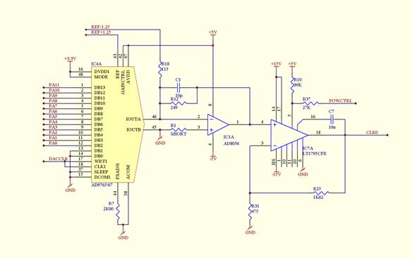
Figur 6: Clock driver cirquit
The
standard driver module ( which is the only one made until now )
contains 6 drivers, each capable of driving the output in the range
-10.00V to
+11.95V at 500mA, 900V/us, and 12bit resolution ( ~5mV/DAU). Se fig 6.
Each
driver consists of a 12bit DAC updated every 10ns ( 100MHz )
feeding an I/V converter with a current bias to generate the bipolar
output.
The bandwidth of the I/V stage is limited to about 30MHz. Finally a
gain and
power stage with the capability of switching the tradeoff between power
consumption and slew rate performance between to levels, - idle and
operating.
This option allows for saving in power, and minimizing heat buildup on
drivers
with low duty cycle ( f.ex. parallel rails). It should be noted that in
a
typical controller setup, about half of the total power consumption is
in the
clock-drivers ( without utilizing the power level switching).
The
12bit input to each DAC as well as the power control bit, are
generated by a sequencer-slave inside a FPGA, one for each driver. The
RAM's
carrying the tables of output waveforms are loaded before the start of
the
readout.
The
patterns can be generated by the local processor or kept in the host
PC and upload when needed. There is no limits of the content, - any
waveform, -
RC-exponential-, constant current slopes-, sine- or
squarewave can be generated independently on
all clocks.

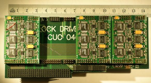
Figur
7: Clock carrier board, mounted with 3 clock driver modules to give a
total of
18 clocks. High speed analog cirquits consumes a lot of power. The
three
modules consumes 12W, or half of the total controller power input. The
driver
modules show the 'analog side' of the boards. The 'FPGA side' supplying
6 x 12
bits to the DAC's is hidden below.


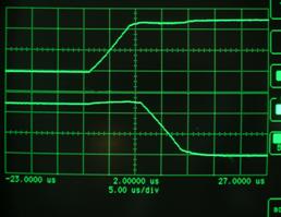
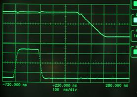
Figur
8: Examples of the programmability of the clock drivers, (left) showing
rg-serial clock relationship during serial clocking, and (right) two
parallel
clocks during parallel clocking. Note the constant current slopes, and
the
effects on the on-chip capacitive couplings. It is the same clock
drivers
generating the waveforms in both pictures.
bulky
charge storage capacitors. The fundamental frequency is phase-locked with the pixel readout.