power supply
sequencer/uP-board
clock-drivers
dewar interface board (DIB)
CCD3-Camera Controller
In the
CCD3 controller, all electronics is integrated in a single box some
18x13x7cm
in size. The primary functional boards, - power
supply, sequencer/uP-board, clock-drivers and video-board are interconnected through a
PC104 based
bus. A dewar interface board (DIB) is the
electrical
and mechanical interface between the controller-boards and the
environment, -
usually the DIB makes it possible to clamp the controller box directly
onto the
dewar.

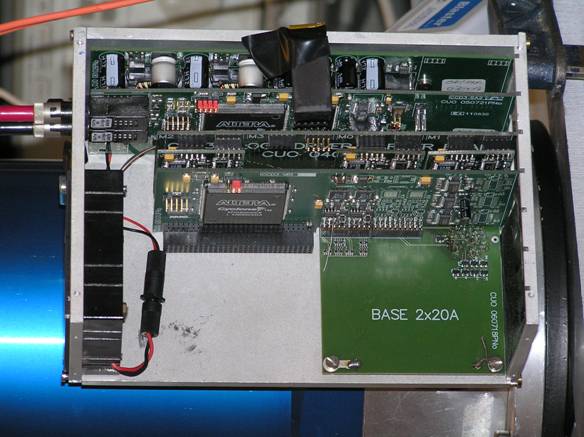
Figur 1 Controller
interior showing a 2-channel,18clock setup
Limiting
the number of channels to 16 and number of clocks to 96, and removing
the mains
supply (220VAC to 24VDC) to a camera support box, makes it possible to
make the
controller small low power ( 18x13x7cm, ~24W for 2 channels), without
any
interconnecting wires
1.1
Fundamentals of operation.
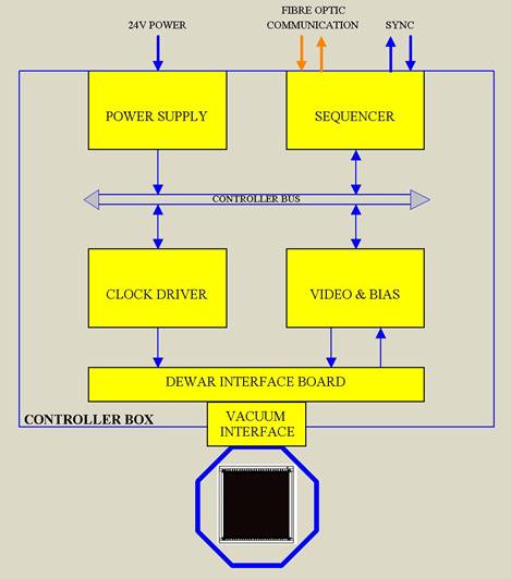
The layout
of the electronics, see fig.3, -
is fairly traditional with a -
·
sequencer
board
taking care of general control, sequencing, communication and
syncronization
·
clock
carrier board with up to 4 clock driver modules. 3 types of modules are
foreseen, - normal CCD clocks, - L3 high voltage clocks and SWIR logic
level
clocks.
·
Video
board containing the electronics for biases and video chains for 4
video-channels
·
Power
supply board, converting a 24VDC input to the power rails needed
·
Dewar
interface board, containing the wiring neccesary to connect the
standard
outputs of the clock- and video-boards to the connector type of the
dewar. It
also contains device protection- and decoupling- cirquitry.

Figur 2 Controller
Overview
In
order to obtain a high speed and time resolution,
without excess increase in power consumption, and without sacrificing
flexibility or performance ( like linearity ), as much as possible of
the
traditional analog cirquitry has been moved into the digital domain.
Two
examples:
In the clock
drivers the waveforms are
generated by feeding 12bit/100MHz digital patterns to a DAC, that
through an
I/V-converter and power-amp is driving the output. Any waveform can be
produced!
In the videochains
the input from the
detector is fed to an amplifier that makes the traditional conversion
of signal
level and impedance, but in this case with an input bandwidth of about
25MHz,
and with the output digitized at 100MHz to 14bits ( which is far enough
regarding the noise levels at the higher bandwidth ). The digital
patterns are
fed into a machine that takes every sample, multiply it by a constant
from a
table and add it to an accumulator, which in turn when the pixel is
done is
forwarded to the data-transmitter. Any CDS filter function can be
produced (not
limited to dual-slope or clamp-sample), and any tradeoff between
digital
resolution and speed can be programmed on the fly in front of every
readout.
This is especially usefull when the user is switching between broadband
imaging
where the noise/speed tradeoff is in favor of speed, and spectroscopy
where the
readout-noise is crucial.
Thus, -
every clockdriver and every videochain
needs to be fed by a digital word every 10ns ( 100MHz). Two techniques
are
used to make this work at low power:
Keeping
the amount of data low:
Of
cause the digital words are stored in
memories kept local on the clock-driver/video-boards respectively. To
make
efficient use of the memory space it is noted that a lot of repetition
is
taking place during the readout of an array. Typically all pixels are
treated
equally, all parallel shifts are equal, all serial sweeps are equal
....and so
on. Actually, very few fundamental sequences are neccesary to describe
any
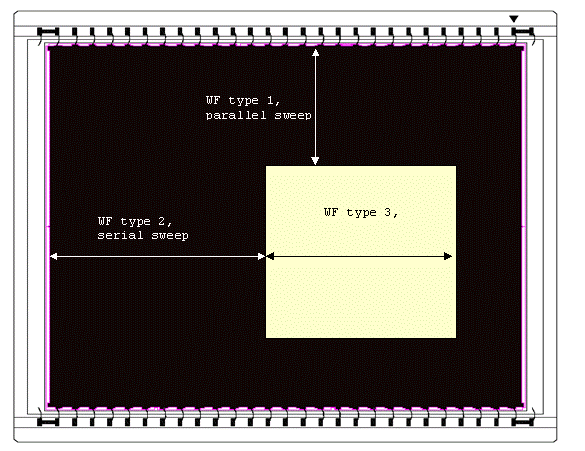
readout. See fig
 Fig. 4: WF example
Keeping
the lines short or simple:
The
function of housekeeping the addresses for
the memories is split into a master function local on the sequencer
board, and a
slave function local on every clock-driver and video-chain.
The
master function is defined by two tables,
one describing the speed properties of each waveform in respect of
length and
clock-prescaling ( used during slow waveforms), and one describing what
the
readout is going to look like in respect
of detector- and image- size, ie. what to do with the waveforms
This
latter table is the actual sequencer, - the table that is stepped
through
during a readout. It is the only table that needs to be modified to
change
image properties like binning and windowing.
The
slave function contains the table of the
datawords fed to the clock-driver DAC's/ CDS-filters respectively, and
a
programmable address generator converting inputs from the master to
actual
addresses. It also contains a setup register that tells each
slave which waveform
type it actually is going to respond to. Typically the serials are
stable during
parallel clocking and vice-versa, as well as the videochains are only
transmitting data during the pixel timing.
The
only signals neccesary to be broadcasted
from the master to make up the interconnect to the slaves are three
high speed
LVDS lines ( clock, clock enable and start of next waveform) and a low
speed
8-bit word telling the value of the next waveform.